 IEEE/ICACT20240052 Slide.07
[Big Slide]
Oral Presentation
| Virual Oral Presentation Slide by Slide |
|
IEEE/ICACT20240052 Slide.07
[Big Slide]
| Oral Presentation |
|
|
|
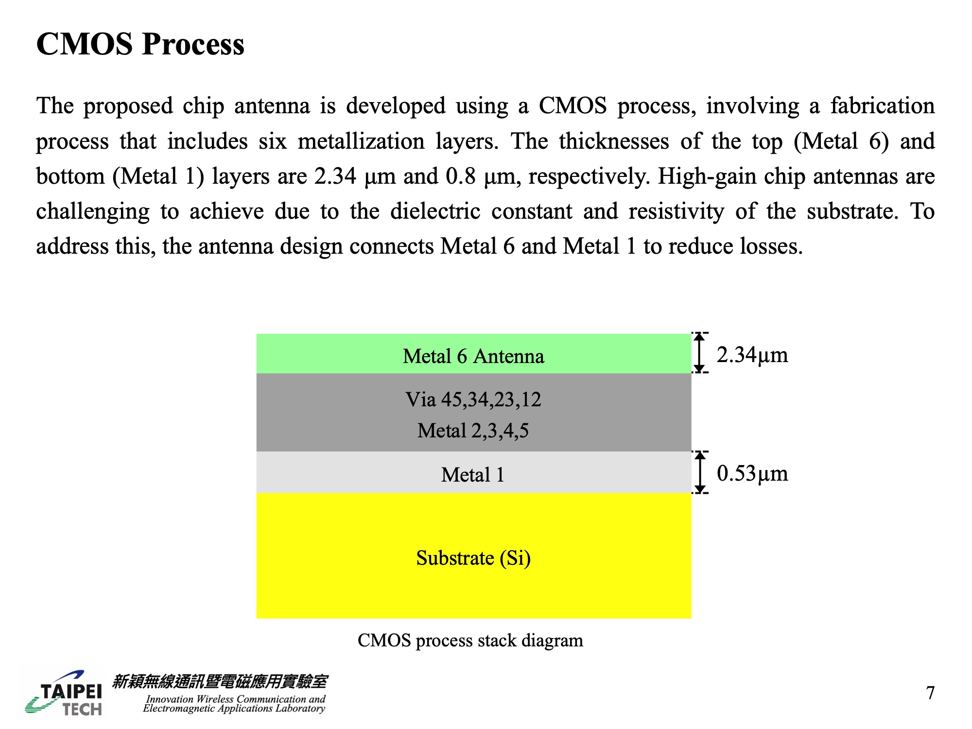
The proposed chip antenna is developed using a CMOS process, involving a fabrication process that includes six metallization layers. The thicknesses of the top (Metal 6) and bottom (Metal 1) layers are 2.34 ¥ìm and 0.8 ¥ìm, respectively. High-gain chip antennas are challenging to achieve due to the dielectric constant and resistivity of the substrate. To address this, the antenna design connects Metal 6 and Metal 1 to reduce losses. | |
| [Go to Next Slide] |