 |
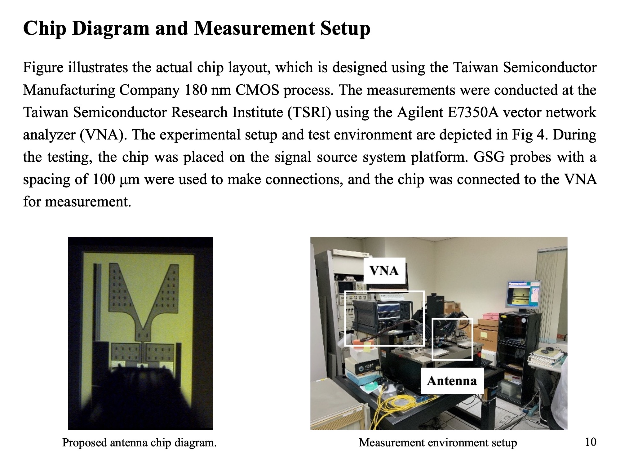
In our experimental setup, we utilized the advanced facilities at Taiwan Semiconductor Research Institute. The chip, fabricated using Taiwan Semiconductor Manufacturing Company's 180 nm CMOS process, underwent thorough testing. The measurements were conducted at the Taiwan Semiconductor Research Institute (TSRI) using the Agilent E7350A vector network analyzer (VNA). The experimental setup and test environment are depicted in Fig 4. During the testing, the chip was placed on the signal source system platform. GSG probes with a spacing of 100 ¥ìm were used to make connections, and the chip was connected to the VNA for measurement. |
 IEEE/ICACT20240052 Slide.10
[Big Slide]