ICACT20210161 Slide.01
[Big Slide] |
Chrome  Click!! |
 |
Good morning, my name is Angie Teo and I am from Brunei Darussalam. Today I will be presenting a topic on Transverse Electric (TE) and Transverse Magnetic (TM) Modes Dependent Effective Index Analysis for a Nano-scale Silicon Waveguide. |
| ICACT20210161 Slide.02
[Big Slide]
|
Chrome Click!! |
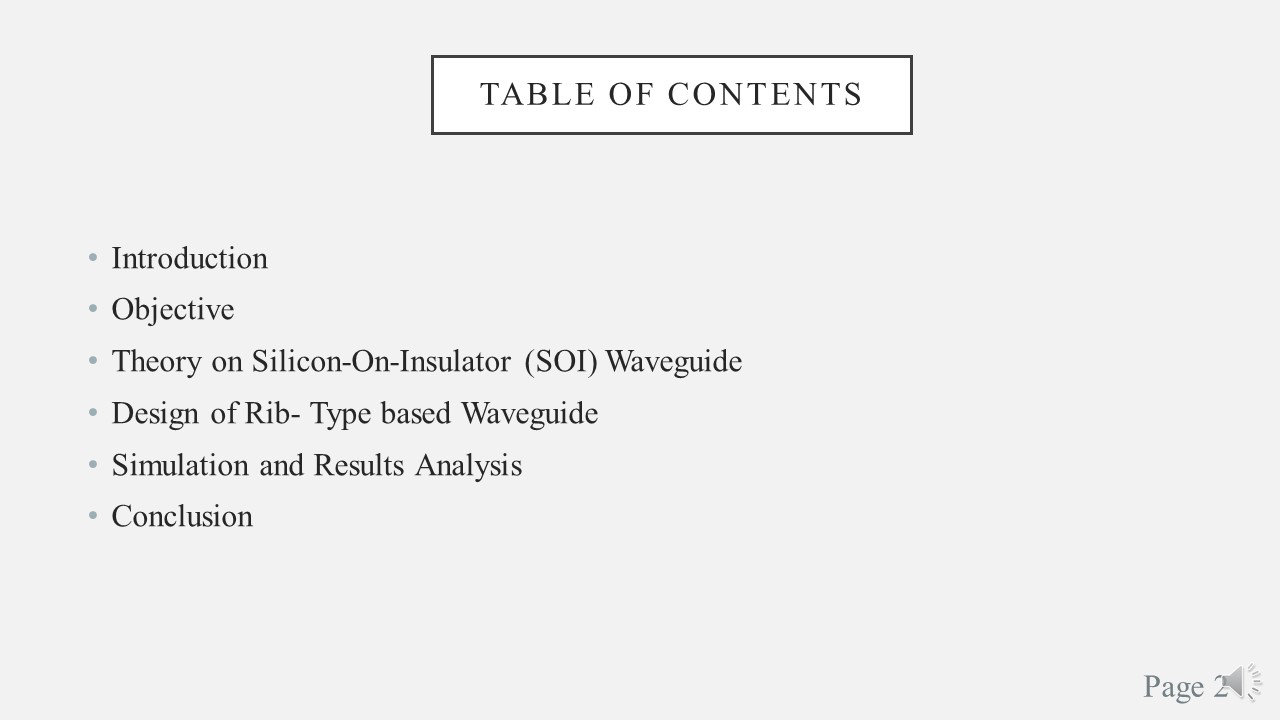 |
Table of contents. Today I will be touching on the introduction, objective, theory on silicon-on-insulator (SOI) waveguide, the design of rib- type based waveguide, simulation and results analysis and lastly, the conclusion. |
| ICACT20210161 Slide.03
[Big Slide]
|
Chrome Click!! |
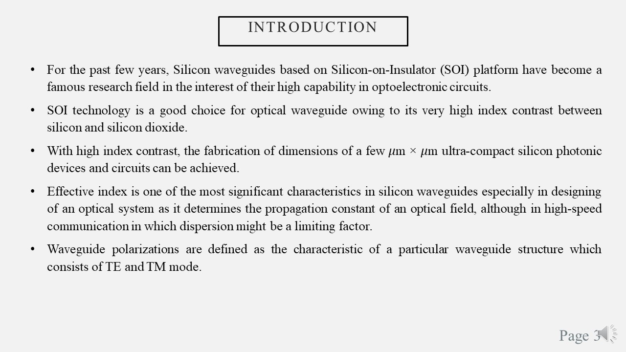 |
Before I get into my main design, let us have some idea on what it is all about. For the past few years, Silicon waveguides based on Silicon-on-Insulator (SOI) platform have become a famous research field in the interest of their high capability in optoelectronic circuits.
SOI technology is a good choice for optical waveguide owing to its very high index contrast between silicon and silicon dioxide.
With high index contrast, the fabrication of dimensions of a few 𝜇m ¡¿ 𝜇m ultra-compact silicon photonic devices and circuits can be achieved.
Effective index is one of the most significant characteristics in silicon waveguides especially in designing of an optical system as it determines the propagation constant of an optical field, although in high-speed communication in which dispersion might be a limiting factor.
Waveguide polarizations are defined as the characteristic of a particular waveguide structure which consists of TE and TM mode. TE is transverse electric and TM is transverse magnetic.
|
| ICACT20210161 Slide.04
[Big Slide]
|
Chrome Click!! |
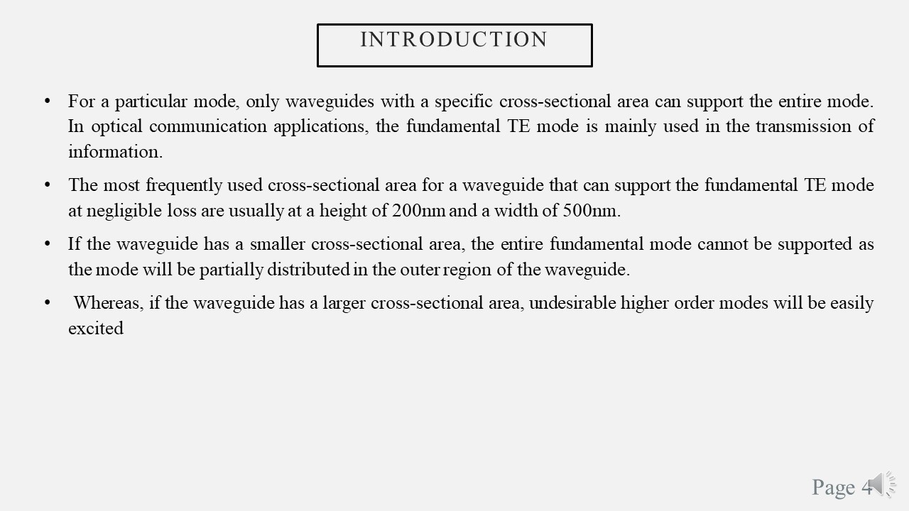 |
For a particular mode, only waveguides with a specific cross-sectional area can support the entire mode. In optical communication applications, the fundamental TE mode is mainly used in the transmission of information.
The most frequently used cross-sectional area for a waveguide that can support the fundamental TE mode at negligible loss are usually at a height of 200nm and a width of 500nm.
If the waveguide has a smaller cross-sectional area, the entire fundamental mode cannot be supported as the mode will be partially distributed in the outer region of the waveguide.
Whereas, if the waveguide has a larger cross-sectional area, undesirable higher order modes will be easily excited.
|
| ICACT20210161 Slide.05
[Big Slide]
|
Chrome Click!! |
 |
The objective of my work is to demonstrate the simulation and analysis of the effect of effective index on silicon waveguide thickness for two different fixed core height which is at 220nm and 200nm, and with each the core width was from 300nm to 600nm at the steps of 100nm for Transverse Electric (TE) and Transverse Magnetic (TM) Mode. |
| ICACT20210161 Slide.06
[Big Slide]
|
Chrome Click!! |
 |
Next, is the theory on silicon-on-insulator rib waveguide.
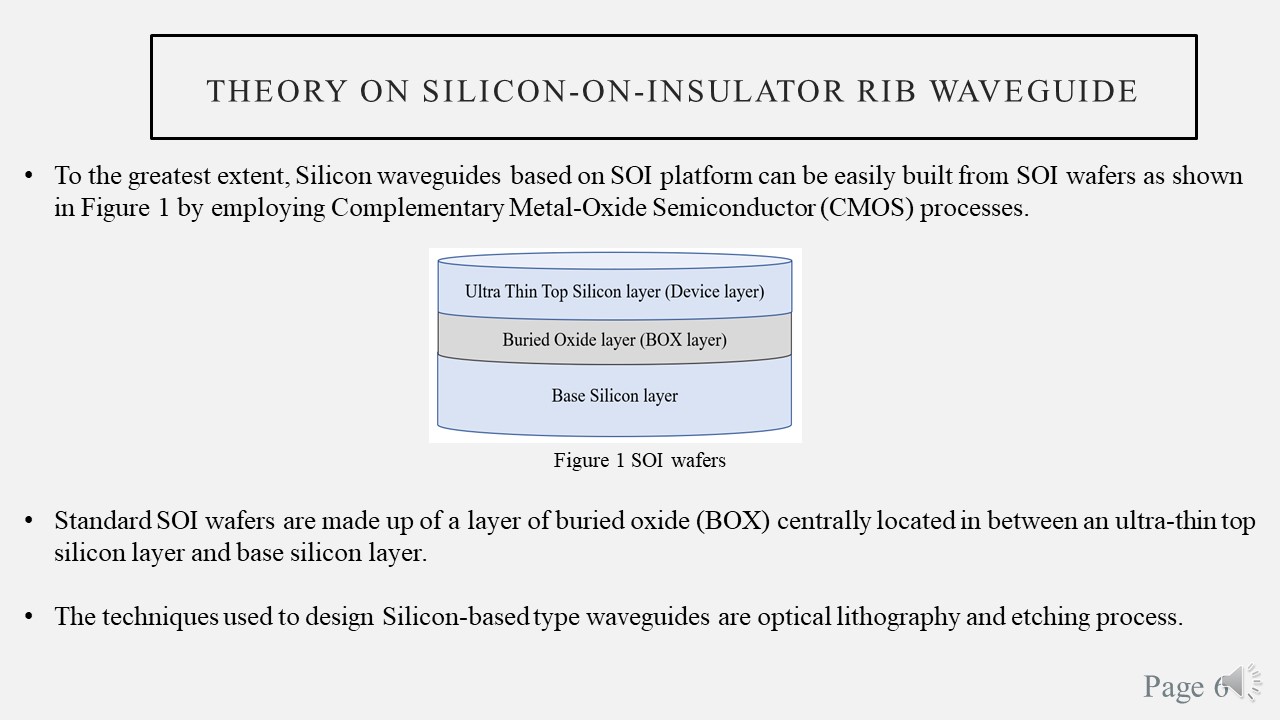
To the greatest extent, silicon waveguides based on SOI platform can be easily built from SOI wafers as shown in Figure 1 by employing complementary metal-oxide semiconductor (CMOS) processes.
So Figure 1 show the SOI wafers. If you see we got the outer ultra-thin silicone layer, buried oxide layer and the base silicone layer.
Standard SOI wafers are made up of a layer of buried oxide (BOX) centrally located in between an ultra-thin top silicon layer and base silicon layer.
The techniques used to design silicon-based type waveguides are optical lithography and etching process.
|
| ICACT20210161 Slide.07
[Big Slide]
|
Chrome Click!! |
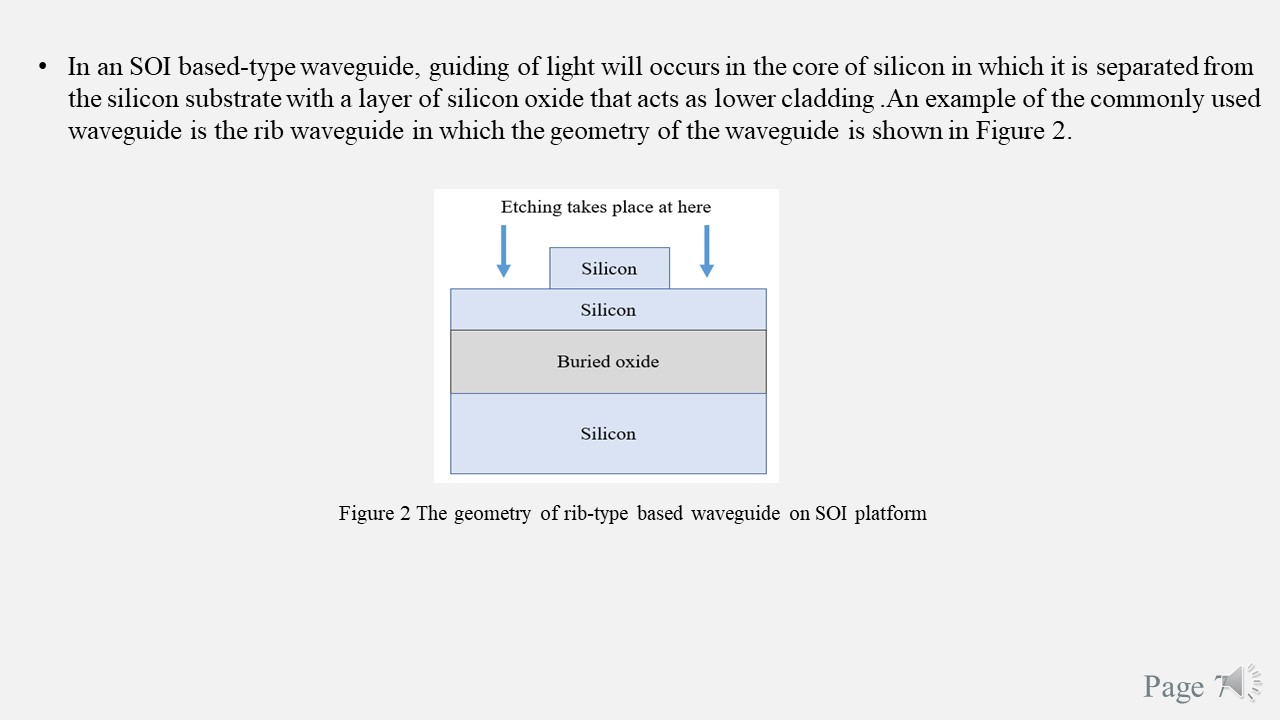 |
In an SOI based-type waveguide, guiding of light will occurs in the core of silicon in which it is separated from the silicon substrate with a layer of silicon oxide that acts as lower cladding.
An example of the commonly used waveguide is the rib waveguide in which the geometry of the waveguide is shown in Figure 2.
So, from Figure 2 you can see that etching takes place as shown from the arrow. |
| ICACT20210161 Slide.08
[Big Slide]
|
Chrome Click!! |
 |
Now, let us look at my design of rib-type based waveguide.
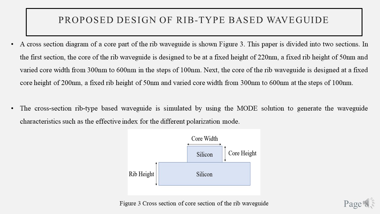
A cross section diagram of a core part of the rib waveguide is shown Figure 3.
This paper is divided into two sections.
In the first section, the core of the rib waveguide is designed to be at a fixed height of 220nm, a fixed rib height of 50nm and varied core width from 300nm to 600nm in the steps of 100nm.
Next, the core of the rib waveguide is designed at a fixed core height of 200nm, a fixed rib height of 50nm and varied core width from 300nm to 600nm at the steps of 100nm.
The cross-section rib-type based waveguide is simulated by using the MODE solution in order to generate the waveguide characteristics such as the effective index for the different polarization mode.
|
| ICACT20210161 Slide.09
[Big Slide]
|
Chrome Click!! |
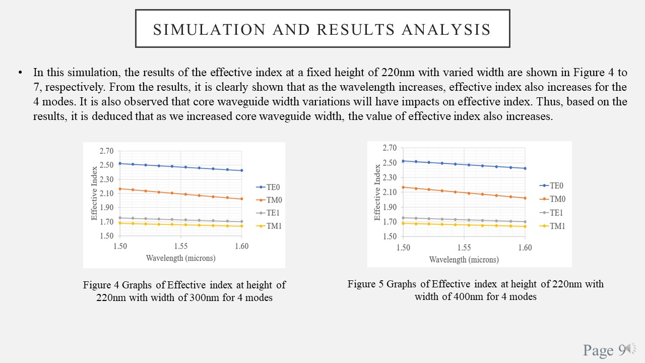 |
The proposed design from previous slide is simulated and the results are obtained.
Results of the effective index at a fixed height of 220nm with varied width are shown in Figure 4 to 7, respectively.
From the results, It is clearly shown that as the wavelength increases, effective index also increases for the 4 modes.
It is also observed that core waveguide width variations will have impacts on effective index.
Thus, based on the results, it is deduced that as we increased core waveguide width, the value of effective index also increases.
Why do we need to have high effective index? This is because high effective index will leads to higher confinement of light.
So this is important In order to design a device with good characteristics such as high effective index.
|
| ICACT20210161 Slide.10
[Big Slide]
|
Chrome Click!! |
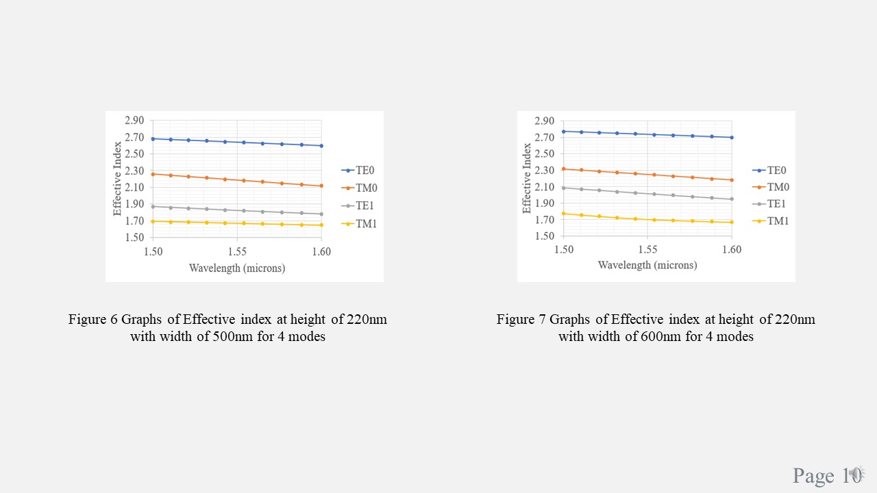 |
Figure 6 shows the graphs of effective index at height of 220nm with width of 500nm whereas for Figure 7 , it is for width of 600nm.
From both Figure, it is shown that as we increased the core width, effective index also increases. |
| ICACT20210161 Slide.11
[Big Slide]
|
Chrome Click!! |
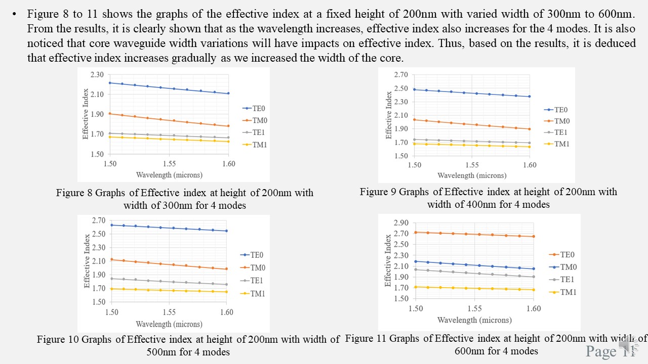 |
Figure 8 to 11 shows the graphs of the effective index at a fixed height of 200nm with varied width of 300nm to 600nm.
From the results, it is clearly shown that as the wavelength increases, effective index also increases for the 4 modes.
It is also noticed that core waveguide width variations will have impacts on effective index.
Thus, based on the results, it is deduced that effective index increases gradually as we increased the width of the core. |
| ICACT20210161 Slide.12
[Big Slide]
|
Chrome Click!! |
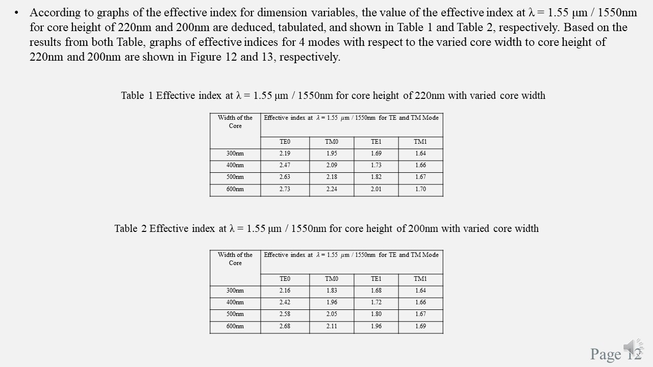 |
So from the Table, it is clearly shown that as we increased the core width, effective index also increases.
As we compared the effective index value for fundamental mode and higher order mode.
The effective index at fundamental mode is higher than higher order mode. |
| ICACT20210161 Slide.13
[Big Slide]
|
Chrome Click!! |
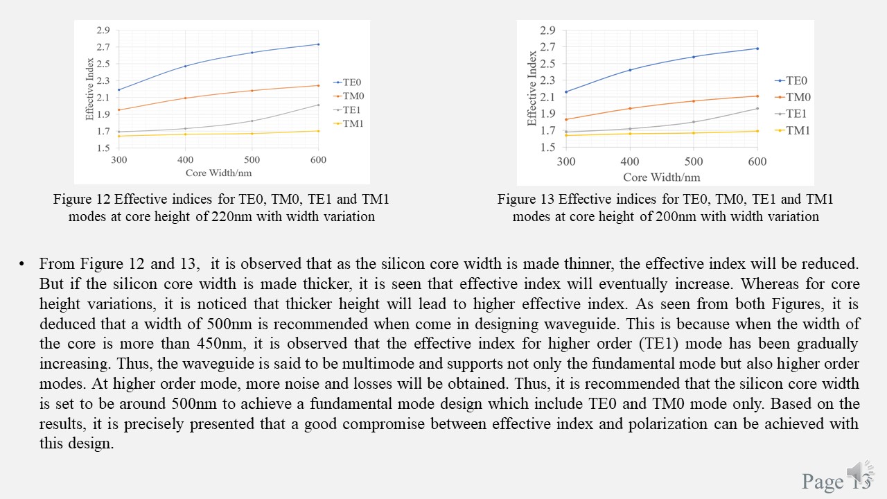 |
And lastly, from Figure 12 and 13, it is observed that as the silicon core width is made thinner, the effective index will be reduced.
But if the silicon core width is made thicker, it is seen that effective index will eventually increase.
Whereas for core height variations, it is noticed that thicker height will lead to higher effective index.
As seen from both Figures, it is deduced that a width of 500nm is recommended when come in designing waveguide.
This is because when the width of the core is more than 450nm, it is observed that the effective index for higher order (TE1) mode has been gradually increasing.
Thus, the waveguide is said to be multimode and supports not only the fundamental mode but also higher order modes.
At higher order mode, more noise and losses will be obtained.
Thus, it is recommended that the silicon core width is set to be around 500nm to achieve a fundamental mode design which include TE0 and TM0 mode only.
Based on the results, it is precisely presented that a good compromise between effective index and polarization can be achieved with this design. |
| ICACT20210161 Slide.14
[Big Slide]
|
Chrome Click!! |
 |
And here, come to our end, two different fixed core height of 220nm and 200nm, respectively, with varied core width of 300nm to 600nm at the steps of 100nm are presented in both TE and TM MODE.
Based on the simulation results, we can clearly see the impact of each design parameters on effective index.
It is seen that with a thicker silicon core height and core width, higher effective index can be achieved.
By analyzing the graphs of effective indices for 4 modes, the determination of fundamental or higher order mode can be accomplished.
From the simulation results, it is clearly observed that TE polarization mode has a much higher effective index than TM polarization.
From the analysis of both graphs, it is seen that as the silicon core width with a value greater than 450nm will easily excite undesirable higher-order modes and may results in more noise and losses. |
| ICACT20210161 Slide.15
[Big Slide]
|
Chrome Click!! |
 |
Thus, it is deduced that silicon core width is recommended to be set at around 500nm in order to achieve a good compromise between effective index and polarizations.
The desired core width is chosen to be at 500nm as the entire fundamental mode cannot be supported at a smaller dimension while undesirable higher mode will get easily excited at a larger dimension. Based on the simulation results, it is concluded that the impact of each design parameters will lead to huge effect on the value of effective index. |
| ICACT20210161 Slide.16
[Big Slide]
|
Chrome Click!! |
 |
Thank You |