ICACT20240052 Slide.00
[Big Slide]
[YouTube] |
Chrome  Click!! |
 |
Good day everyone. I am Ming-Chun Hsieh from the National Taipei University of Technology. I'm honored to present our latest research on 'Chip Antenna with Vivaldi-Like Structure for W-Band Design'. This work is a collaborative effort from our team at the Innovation Wireless Communication and Electromagnetic Applications Laboratory.
|
| ICACT20240052 Slide.01
[Big Slide]
|
Chrome Click!! |
 |
Our presentation will unfold in four key segments. Initially, I will introduce the context and significance of our study. Next, I'll delve into the specifics of our antenna design, followed by a detailed discussion of our results. Lastly, we'll touch upon relevant references that have guided our research. |
| ICACT20240052 Slide.02
[Big Slide]
|
Chrome Click!! |
 |
Introdcution |
| ICACT20240052 Slide.03
[Big Slide]
|
Chrome Click!! |
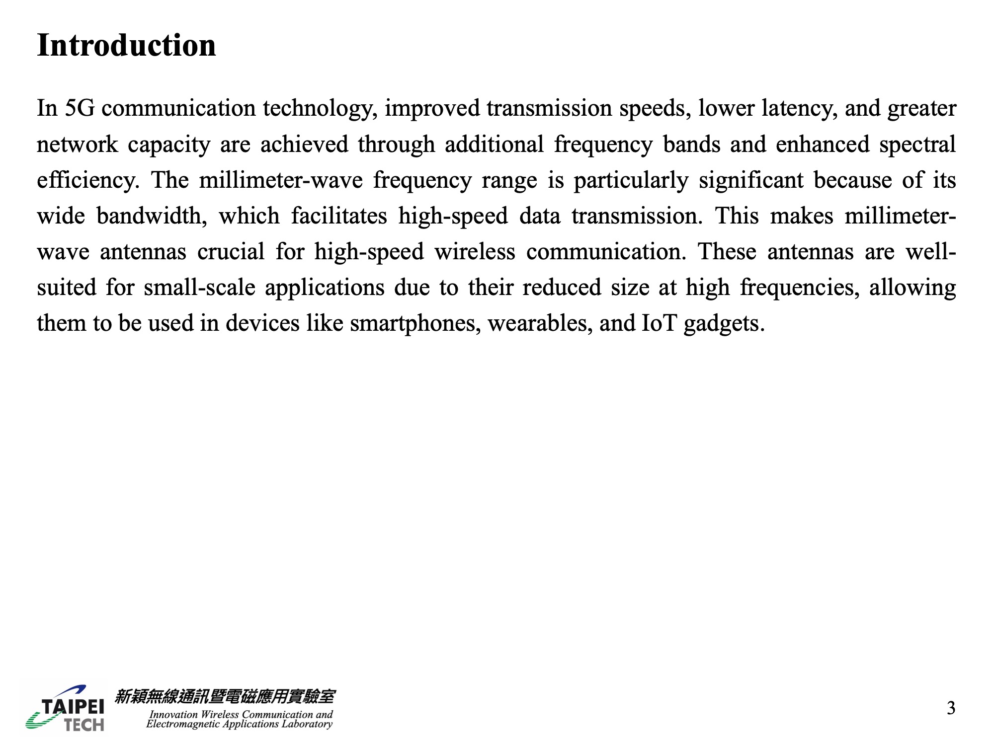 |
In the dynamic landscape of 5G communication, the quest for improved transmission speeds, reduced latency, and expanded network capacity is incessant. The millimeter-wave frequency range emerges as a pivotal aspect, thanks to its extensive bandwidth that enables rapid data transmission. This makes the development of efficient millimeter-wave antennas indispensable for the future of wireless communication. |
| ICACT20240052 Slide.04
[Big Slide]
|
Chrome Click!! |
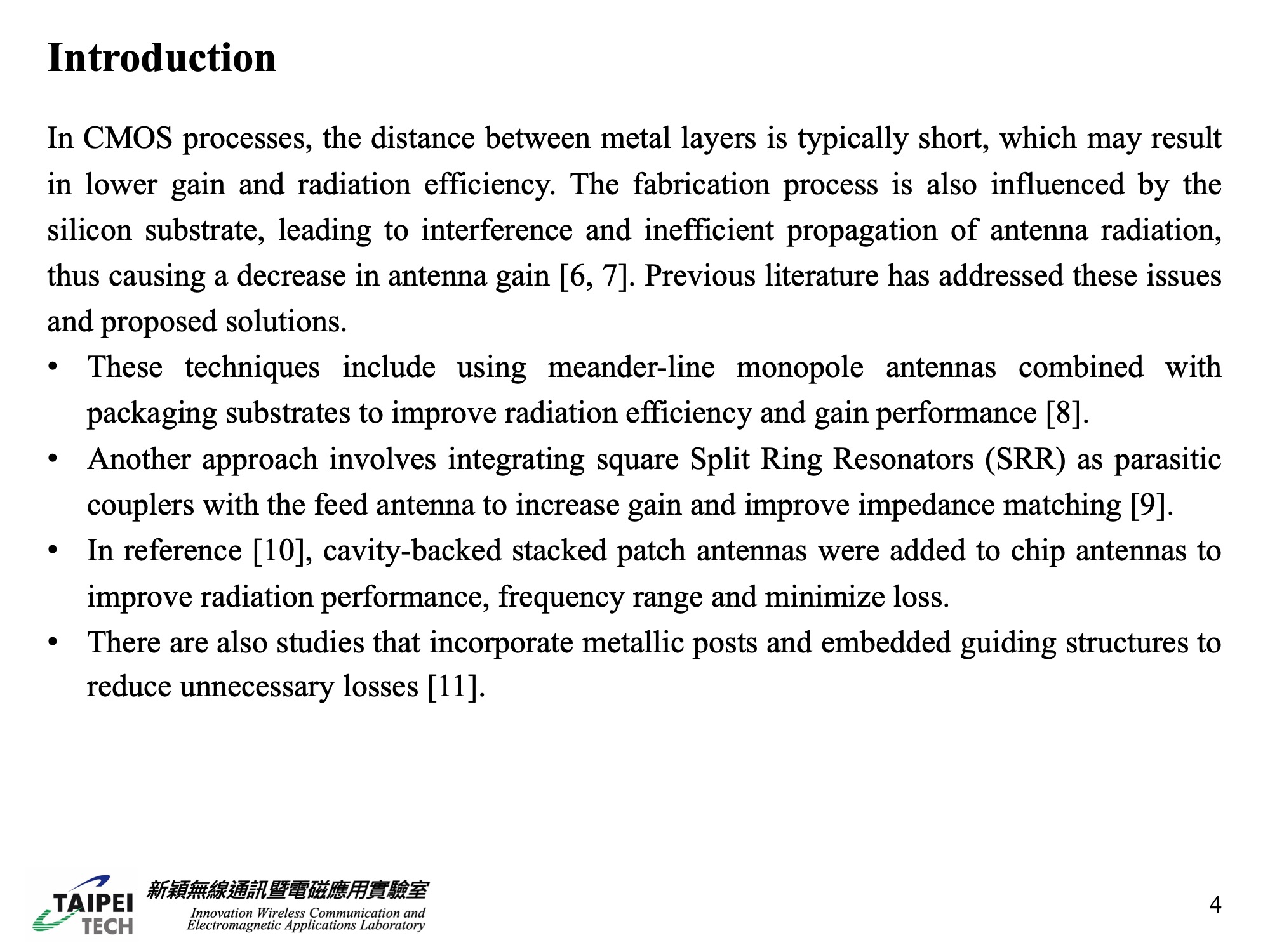 |
In the domain of CMOS antenna design, we encounter a critical challenge: the proximity of metal layers which can lead to suboptimal gain and radiation efficiency. Not to overlook, the fabrication process itself, influenced by the silicon substrate, could introduce interference, detracting from the efficacy of antenna radiation. The literature reflects a continued effort to surmount these hurdles.
For instance, one method has involved the fusion of meander-line monopole antennas with packaging substrates to boost radiation efficiency and augment gain. Moreover, incorporating square Split Ring Resonators as parasitic couplers with the feed antenna has proven beneficial in enhancing gain and refining impedance matching. The literature also cites the implementation of cavity-backed stacked patch antennas, which have served to amplify radiation performance and broaden the frequency range while curbing losses.
Our presentation also showcases a variety of other methods and strategies, reflecting the breadth and depth of research in this evolving field.
|
| ICACT20240052 Slide.05
[Big Slide]
|
Chrome Click!! |
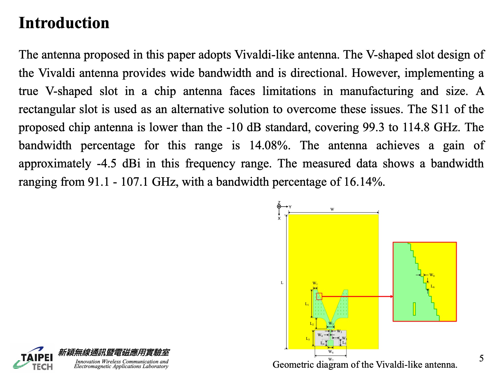 |
In our study, we propose an antenna that integrates the advantages of a Vivaldi-like design. This approach addresses the manufacturing and size constraints of traditional V-shaped slots, using a rectangular slot as a viable alternative. The S11 of the proposed chip antenna is lower than the -10 dB standard, covering 99.3 to 114.8 GHz. The bandwidth percentage for this range is 14.08%. The antenna achieves a gain of approximately -4.5 dBi in this frequency range. The measured data shows a bandwidth ranging from 91.1 - 107.1 GHz, with a bandwidth percentage of 16.14%. |
| ICACT20240052 Slide.06
[Big Slide]
|
Chrome Click!! |
 |
Antenna Design |
| ICACT20240052 Slide.07
[Big Slide]
|
Chrome Click!! |
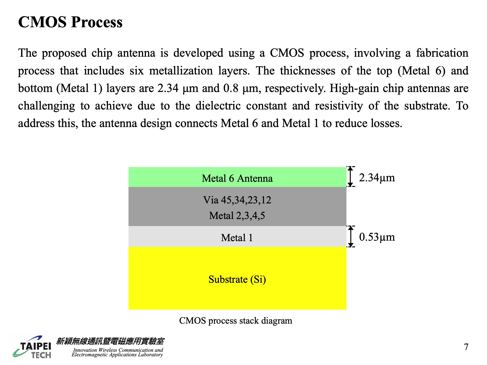 |
The proposed chip antenna is developed using a CMOS process, involving a fabrication process that includes six metallization layers. The thicknesses of the top (Metal 6) and bottom (Metal 1) layers are 2.34 μm and 0.8 μm, respectively. High-gain chip antennas are challenging to achieve due to the dielectric constant and resistivity of the substrate. To address this, the antenna design connects Metal 6 and Metal 1 to reduce losses. |
| ICACT20240052 Slide.08
[Big Slide]
|
Chrome Click!! |
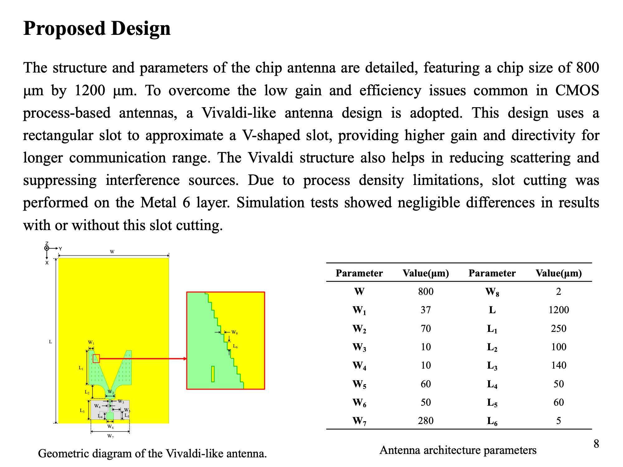 |
The structure and parameters of the chip antenna are detailed, featuring a chip size of 800 μm by 1200 μm. To overcome the low gain and efficiency issues common in CMOS process-based antennas, a Vivaldi-like antenna design is adopted. This design uses a rectangular slot to approximate a V-shaped slot, providing higher gain and directivity for longer communication range. The Vivaldi structure also helps in reducing scattering and suppressing interference sources. Due to process density limitations, slot cutting was performed on the Metal 6 layer. Simulation tests showed negligible differences in results with or without this slot cutting. |
| ICACT20240052 Slide.09
[Big Slide]
|
Chrome Click!! |
 |
Result |
| ICACT20240052 Slide.10
[Big Slide]
|
Chrome Click!! |
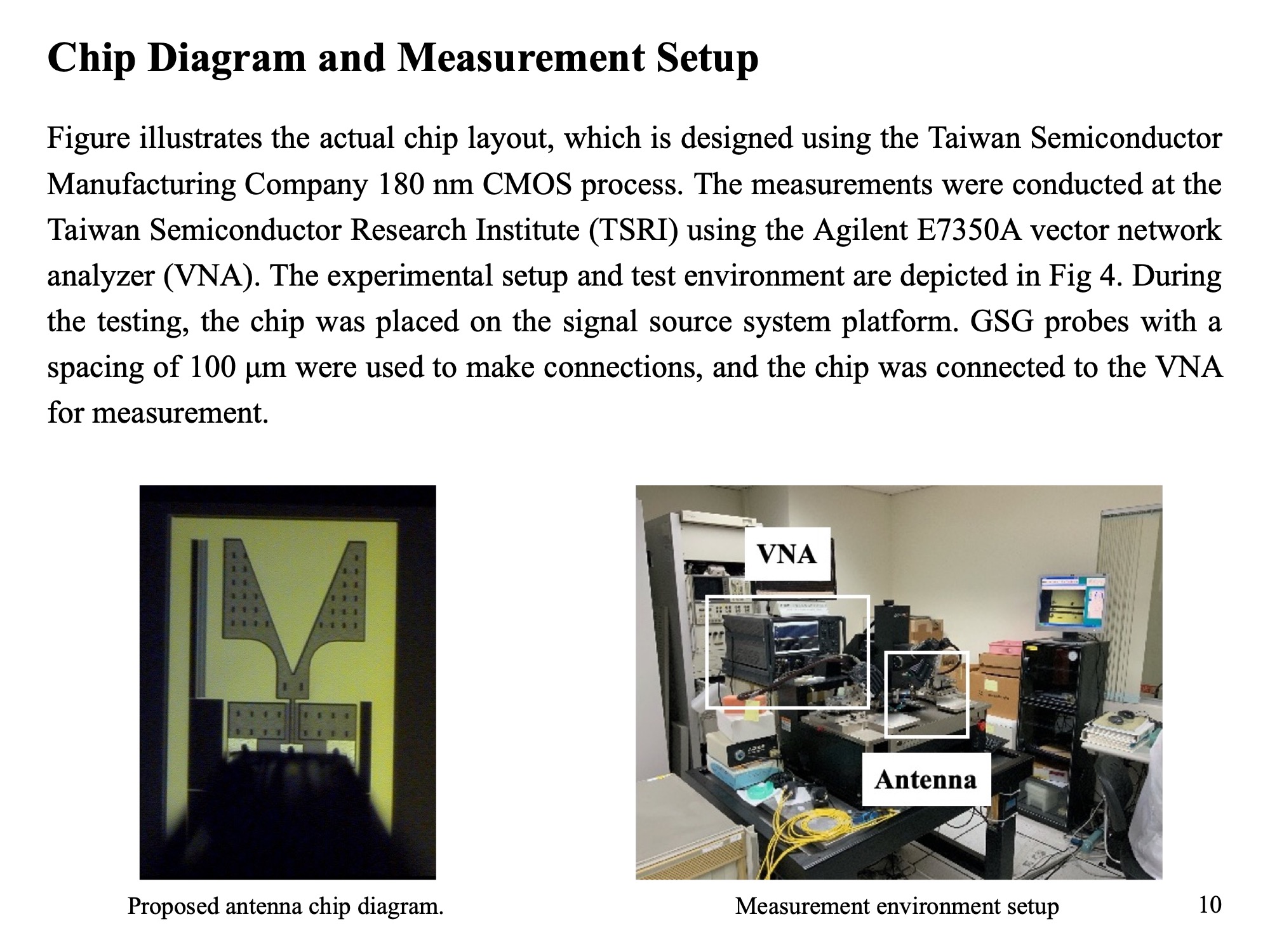 |
In our experimental setup, we utilized the advanced facilities at Taiwan Semiconductor Research Institute. The chip, fabricated using Taiwan Semiconductor Manufacturing Company's 180 nm CMOS process, underwent thorough testing. The measurements were conducted at the Taiwan Semiconductor Research Institute (TSRI) using the Agilent E7350A vector network analyzer (VNA). The experimental setup and test environment are depicted in Fig 4. During the testing, the chip was placed on the signal source system platform. GSG probes with a spacing of 100 μm were used to make connections, and the chip was connected to the VNA for measurement. |
| ICACT20240052 Slide.11
[Big Slide]
|
Chrome Click!! |
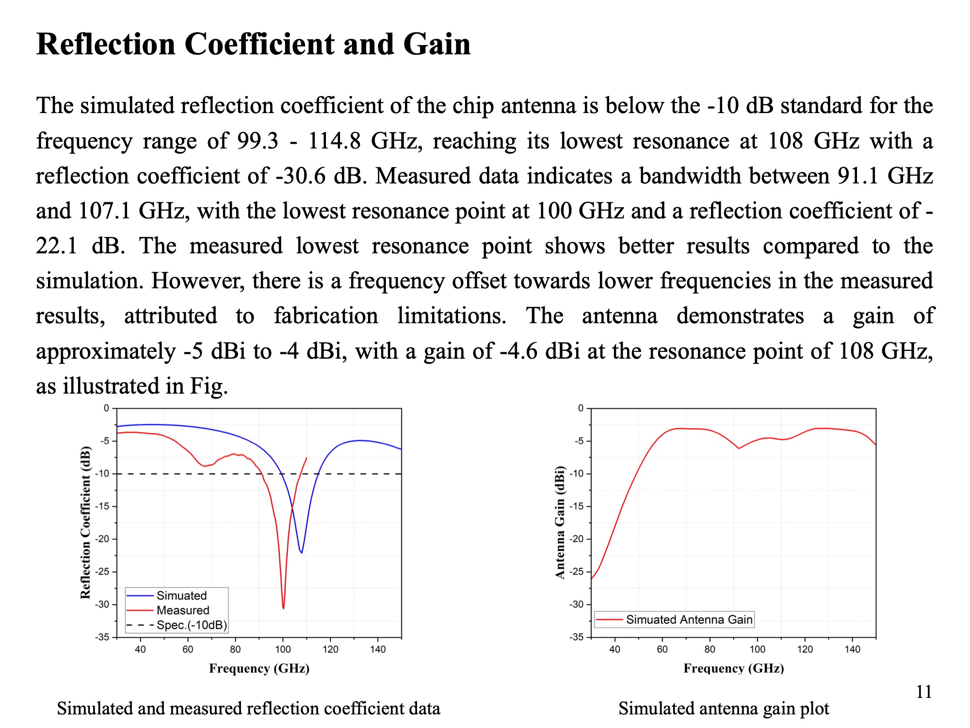 |
The simulated reflection coefficient of the chip antenna is below the -10 dB standard for the frequency range of 99.3 - 114.8 GHz, reaching its lowest resonance at 108 GHz with a reflection coefficient of -30.6 dB. Measured data indicates a bandwidth between 91.1 GHz and 107.1 GHz, with the lowest resonance point at 100 GHz and a reflection coefficient of -22.1 dB. Due to the limitations of the vector network analyzer (VNA) used, which has a frequency range of 2 - 110 GHz, measurements beyond 110 GHz were not possible and are not included in the graph. The measured lowest resonance point shows better results compared to the simulation. However, there is a frequency offset towards lower frequencies in the measured results, attributed to fabrication limitations. Despite this, the overall trend of the measured results closely matches the simulated values, suggesting that the performance beyond 150 GHz would also align with the simulations. The antenna demonstrates a gain of approximately -5 dBi to -4 dBi, with a gain of -4.6 dBi at the resonance point of 108 GHz, as illustrated in Fig. |
| ICACT20240052 Slide.12
[Big Slide]
|
Chrome Click!! |
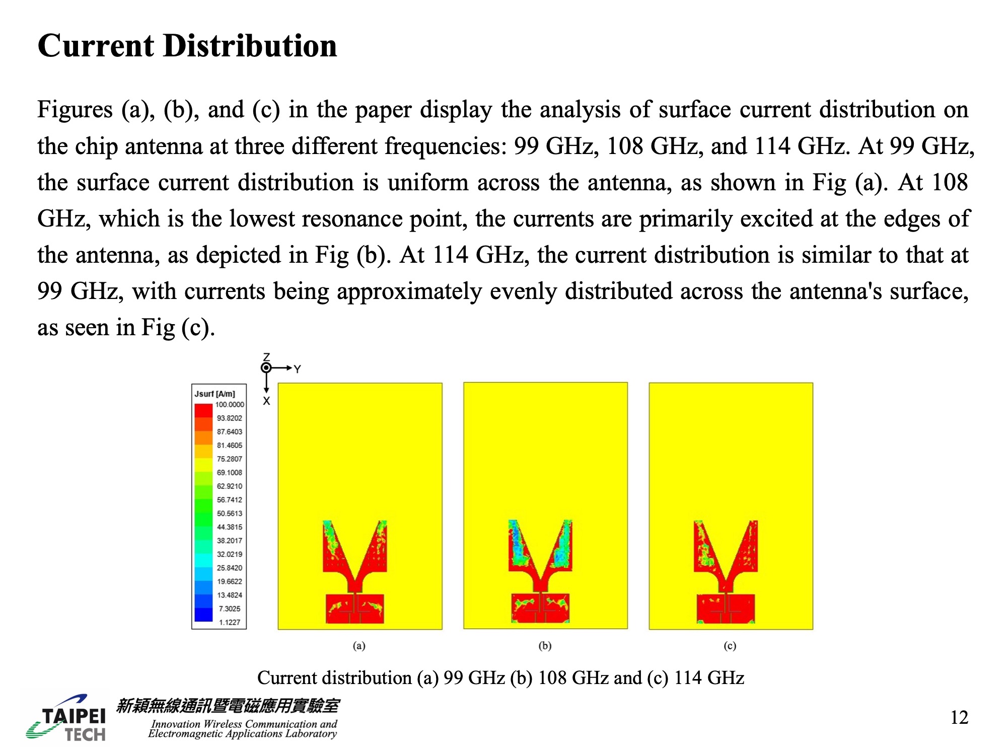 |
In the paper, Figures (a), (b), and (c) illustrate the surface current distribution on the chip antenna at three distinct frequencies: 99 GHz, 108 GHz, and 114 GHz. Figure (a) shows that at 99 GHz, the current distribution is even across the antenna. Figure (b) depicts the situation at 108 GHz, the antenna's lowest resonance point, where the currents are mainly concentrated at the antenna's edges. Finally, Figure (c) demonstrates that at 114 GHz, the current distribution resembles that at 99 GHz, with the currents being fairly uniformly distributed over the antenna's surface. |
| ICACT20240052 Slide.13
[Big Slide]
|
Chrome Click!! |
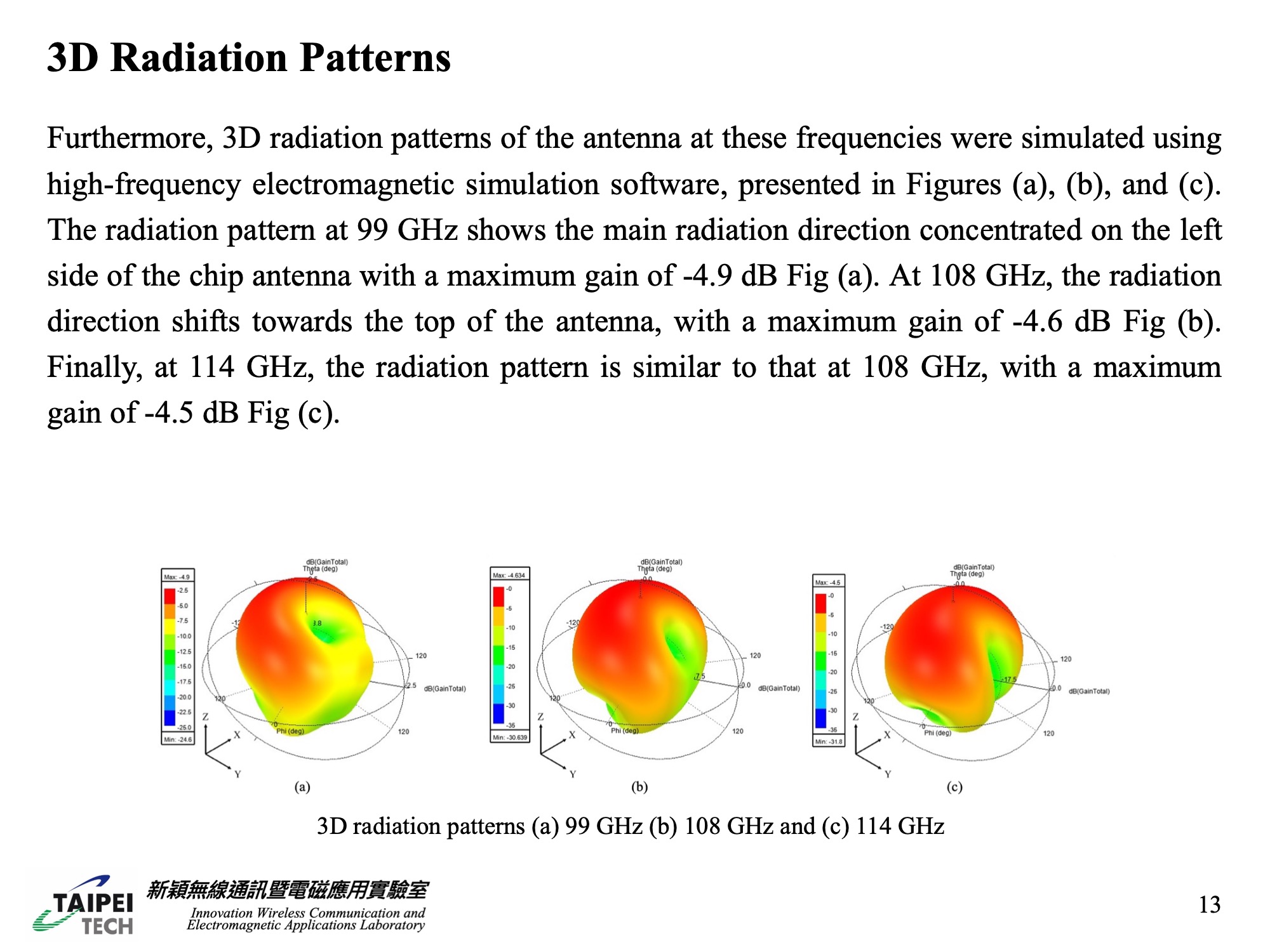 |
3D radiation patterns of the antenna at these frequencies were simulated using high-frequency electromagnetic simulation software, presented in Figures (a), (b), and (c). The radiation pattern at 99 GHz shows the main radiation direction concentrated on the left side of the chip antenna with a maximum gain of -4.9 dB Fig (a). At 108 GHz, the radiation direction shifts towards the top of the antenna, with a maximum gain of -4.6 dB Fig (b). Finally, at 114 GHz, the radiation pattern is similar to that at 108 GHz, with a maximum gain of -4.5 dB Fig (c). |
| ICACT20240052 Slide.14
[Big Slide]
|
Chrome Click!! |
 |
This paper proposes a W-band chip antenna with a Vivaldi-like antenna structure and fabricated in CMOS technology. The size of the chip is 800 μm×1200 μm. In the future, it will be possible to explore the impact of different CMOS processes on chip antennas. By employing different structural designs, it will be feasible to achieve improved performance. |
| ICACT20240052 Slide.16
[Big Slide]
|
Chrome Click!! |
 |
Reference |
| ICACT20240052 Slide.17
[Big Slide]
|
Chrome Click!! |
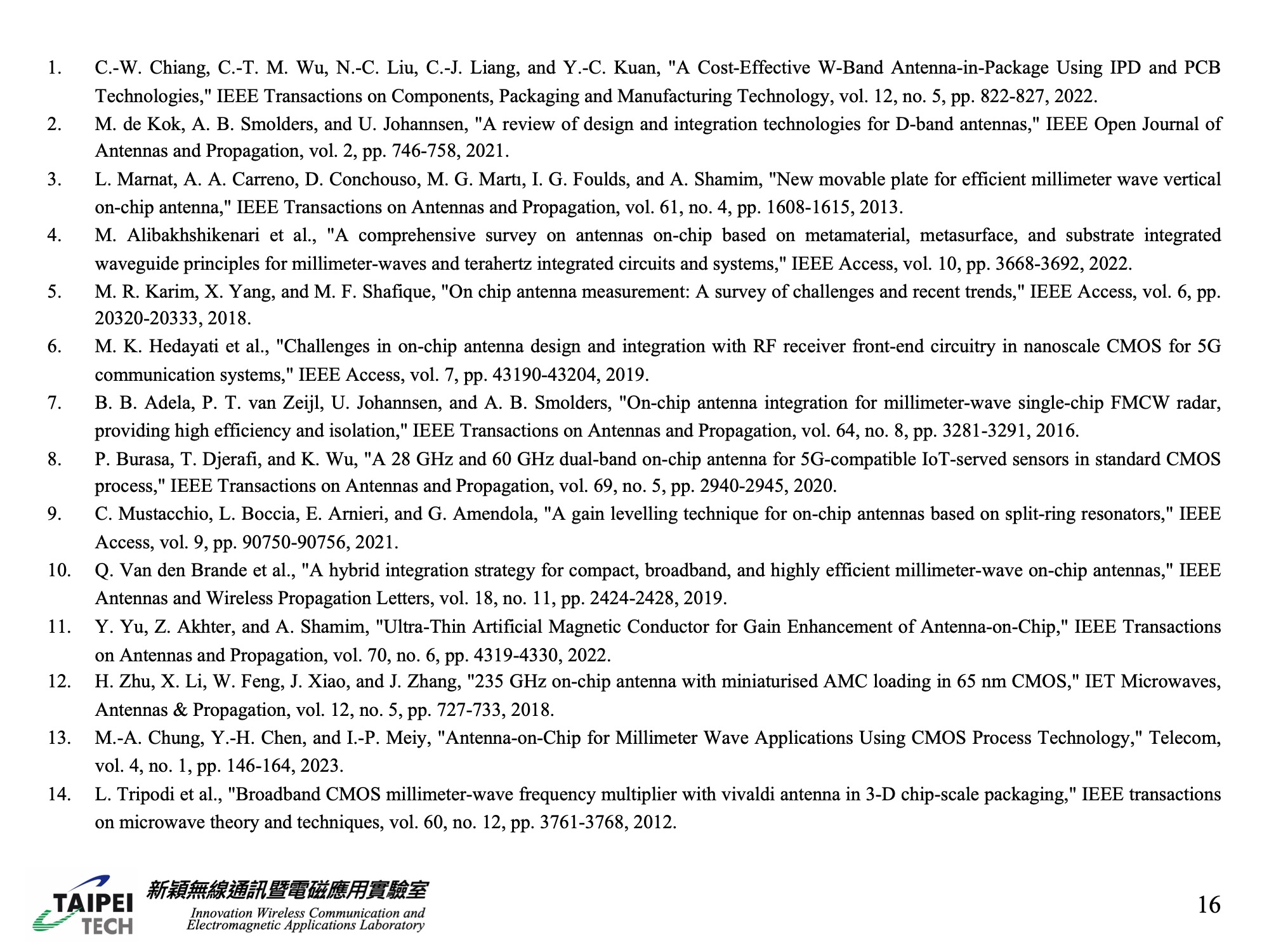 |
This is ours references. |
| ICACT20240052 Slide.18
[Big Slide]
|
Chrome Click!! |
 |
Thanks for listening. |